How to Think About GPUs
Part 12 of How To Scale Your Model (Part 11: Conclusion | The End)
We love TPUs at Google, but GPUs are great too. This chapter takes a deep dive into the world of GPUs – how each chip works, how they're networked together, and what that means for LLMs, especially compared to TPUs. While there are a multitude of GPU architectures from NVIDIA, AMD, Intel, and others, here we will focus on NVIDIA GPUs. This section builds on Chapter 2 and Chapter 5, so you are encouraged to read them first.
What Is a GPU?
A modern ML GPU (e.g. H100, B200) is basically a bunch of compute cores that specialize in matrix multiplication (called Streaming Multiprocessors or SMs) connected to a stick of fast memory (called HBM). Here’s a diagram:
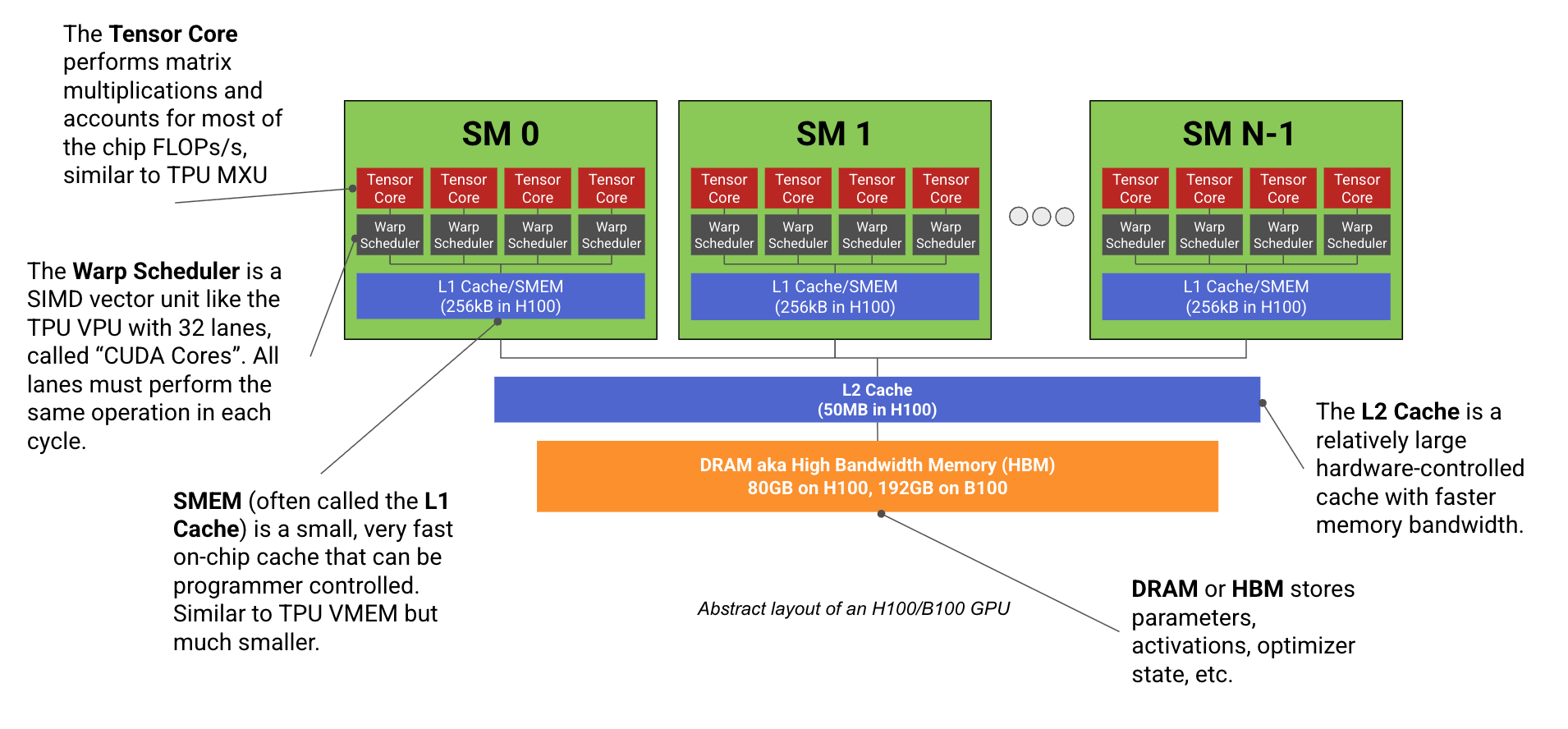
Each SM, like a TPU’s Tensor Core, has a dedicated matrix multiplication core (unfortunately also called a Tensor Core
Let’s take a more detailed view of an H100 SM:
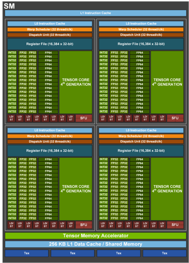
Each SM is broken up into 4 identical quadrants, which NVIDIA calls SM subpartitions, each containing a Tensor Core, 16k 32-bit registers, and a SIMD/SIMT vector arithmetic unit called a Warp Scheduler, whose lanes (ALUs) NVIDIA calls CUDA Cores. The core component of each partition is arguably the Tensor Core, which performs matrix multiplications and makes up the vast majority of its FLOPs/s, but it’s not the only component worth noting.
-
CUDA Cores: each subpartition contains a set of ALUs called CUDA Cores that do SIMD/SIMT vector arithmetic. Each ALU can generally do 1 arithmetic op each cycle, e.g. f32.add.
Newer GPUs support FMA (Fused-Multiply Add) instructions which technically do two FLOPs each cycle, a fact NVIDIA uses ruthlessly to double their reported specs. Each subpartition contains 32 fp32 cores (and a smaller number of int32 and fp64 cores) that all execute the same instruction in each cycle. Like the TPU’s VPU, CUDA cores are responsible for ReLUs, pointwise vector operations, and reductions (sums).Historically, before the introduction of the Tensor Core, the CUDA cores were the main component of the GPU and were used for rendering, including ray-triangle intersections and shading. On today's gaming GPUs, they still do a bulk of the rendering work, while TensorCores are used for up-sampling (DLSS), which allows the GPU to render at a lower resolution (fewer pixels = less work) and upsample using ML. -
Tensor Core (TC): each subpartition has its own Tensor Core, which is a dedicated matrix multiplication unit like a TPU MXU. The Tensor Core represents the vast majority of the GPU’s FLOPs/s (e.g. on an H100, we have 990 bf16 TC TFLOP/s compared to just 66 TFLOPs/s from the CUDA cores).
- 990 bf16 TFLOPs/s with 132 SM running at 1.76GHz means each H100 TC can do
7.5e12 / 1.76e9 / 4 ~ 1024bf16 FLOPs/cycle, roughly an 8x8x8 matmul.NVIDIA doesn't share many TC hardware details, so this is more a guess than definite fact – certainly, it doesn't speak to how the TC is implemented. We know that a V100 can perform 256 FLOPs/TC/cycle. An A100 can do 512, H100 can do 1024, and while the B200 details aren't published, it seems likely it's about 2048 FLOPs/TC/cycle, since `2250e12 / (148 * 4 * 1.86e9)` is about 2048. Some more details are confirmed here. - Like TPUs, GPUs can do lower precision matmuls at higher throughput (e.g. H100 has 2x fp8 FLOPs/s vs. fp16). Low-precision training or serving can be significantly faster.
- Each GPU generation since Volta has increased the TC size over the previous generation (good article on this). With B200 the TC has gotten so large it can no longer fit its inputs in SMEM, so B200s introduce a new memory space called TMEM.
In Ampere, the Tensor Core could be fed from a single warp, while in Hopper it requires a full SM (warpgroup) and in Blackwell it's fed from 2 SMs. The matmuls have also become so large in Blackwell that the arguments (specifically, the accumulator) no longer fit into register memory/SMEM, so Blackwell adds TMEM to account for this.
- 990 bf16 TFLOPs/s with 132 SM running at 1.76GHz means each H100 TC can do
CUDA cores are more flexible than a TPU’s VPU: GPU CUDA cores (since V100) use what is called a SIMT (Single Instruction Multiple Threads) programming model, compared to the TPU’s SIMD (Single Instruction Multiple Data) model. Like ALUs in a TPU’s VPU, CUDA cores within a subpartition must execute the same operation in each cycle (e.g. if one core is adding two floats, then every other CUDA core in the subpartition must also do so). Unlike the VPU, however, each CUDA core (or “thread” in the CUDA programming model) has its own instruction pointer and can be programmed independently. When two threads in the same warp are instructed to perform different operations, you effectively do both operations, masking out the cores that don’t need to perform the divergent operation.

This enables flexible programming at the thread level, but at the cost of silently degrading performance if warps diverge too often. Threads can also be more flexible in what memory they can access; while the VPU can only operate on contiguous blocks of memory, CUDA cores can access individual floats in shared registers and maintain per-thread state.
CUDA core scheduling is also more flexible: SMs run a bit like multi-threaded CPUs, in the sense that they can “schedule” many programs (warps) concurrently (up to 64 per SM) but each Warp Scheduler only ever executes a single program in each clock cycle.
Memory
Beyond the compute units, GPUs have a hierarchy of memories, the largest being HBM (the main GPU memory), and then a series of smaller caches (L2, L1/SMEM, TMEM, register memory).
- Registers: Each subpartition has its own register file containing 16,384 32-bit words on H100/B200 (
4 * 16384 * 4 = 256kiBper SM) accessible by the CUDA cores.- Each CUDA core can only access up to 256 registers at a time, so although we can schedule up to 64 “resident warps” per SM, you can only fit 8 (
256 * 1024 / (4 * 32 * 256)) at a time if each thread uses 256 registers.
- Each CUDA core can only access up to 256 registers at a time, so although we can schedule up to 64 “resident warps” per SM, you can only fit 8 (
-
SMEM (L1 Cache): each SM has its own 256kB on-chip cache called SMEM, which can either be programmer controlled as “shared memory” or used by the hardware as an on-chip cache. SMEM is used for storing activations and inputs to TC matmuls.
- L2 Cache: all SMs share
Technically, the L2 cache is split in two, so half the SMs can access 25MB a piece on an H100. There is a link connecting the two halves, but at lower bandwidth. a relatively large ~50MB L2 cache used to reduce main memory accesses.- This is similar in size to a TPU’s VMEM but it’s much slower and isn’t programmer controlled. This leads to a bit of “spooky action at a distance” where the programmer needs to modify memory access patterns to ensure the L2 cache is well used.
The fact that the L2 cache is shared across all SMs effectively forces the programmer to run the SMs in a fairly coordinated way anyway, despite the fact that, in principle, they are independent units. - NVIDIA does not publish the L2 bandwidth for their chips, but it’s been measured to be about 5.5TB/s. This is roughly 1.6x the HBM bandwidth but it’s full-duplex, so the effective bidirectional bandwidth is closer to 3x. By comparison, a TPU’s VMEM is 2x larger and has much more bandwidth (around 40TB/s).
- This is similar in size to a TPU’s VMEM but it’s much slower and isn’t programmer controlled. This leads to a bit of “spooky action at a distance” where the programmer needs to modify memory access patterns to ensure the L2 cache is well used.
- HBM: the main GPU memory, used for storing model weights, gradients, activations, etc.
- The HBM size has increased a lot from 32GB in Volta to 192GB in Blackwell (B200).
- The bandwidth from HBM to the CUDA Tensor Core is called HBM bandwidth or memory bandwidth, and is about 3.35TB/s on H100 and 9TB/s on B200.
Summary of GPU specs
Here is a summary of GPU specs for recent models. The number of SMs, clock speed, and FLOPs differ somewhat between variants of a given GPU. Here are memory capacity numbers:
| GPU | Generation | Clock Speed | SMs/chip | SMEM capacity/SM | L2 capacity/chip | HBM capacity/chip |
|---|---|---|---|---|---|---|
| V100 | Volta | 1.25GHz/1.38GHz | 80 | 96kB | 6MB | 32GB |
| A100 | Ampere | 1.10GHz/1.41GHz | 108 | 192kB | 40MB | 80GB |
| H100 | Hopper | 1.59GHz/1.98GHz | 132 | 256kB | 50MB | 80GB |
| H200 | Hopper | 1.59GHz/1.98GHz | 132 | 256kB | 50MB | 141GB |
| B200 | Blackwell | ? | 148 | 256kB | 126MB | 192GB |
All generations have 256kB of register memory per SM. Blackwell adds 256kB of TMEM per SM as well. Here are the FLOPs and bandwidth numbers for each chip:
| GPU | Generation | HBM BW/chip | FLOPs/s/chip (bf16/fp16) | FLOPs/s/chip (fp8/int8) | FLOPs/s/chip (fp4) |
|---|---|---|---|---|---|
| V100 | Volta | 9.0e11 | — | — | — |
| A100 | Ampere | 2.0e12 | 3.1e14 | 6.2e14 | — |
| H100 | Hopper | 3.4e12 | 9.9e14 | 2.0e15 | — |
| H200 | Hopper | 4.8e12 | 9.9e14 | 2.0e15 | — |
| B200 | Blackwell | 8.0e12 | 2.3e15 | 4.5e15 | 9.0e15 |
We exclude B100 since it wasn’t mass-produced.
Here’s a helpful cheat sheet comparing GPU and TPU components:
| GPU | TPU | What is it? |
|---|---|---|
| Streaming Multiprocessor (SM) | Tensor Core | Core “cell” that contains other units |
| Warp Scheduler | VPU | SIMD vector arithmetic unit |
| CUDA Core | VPU ALU | SIMD ALU |
| SMEM (L1 Cache) | VMEM | Fast on-chip cache memory |
| Tensor Core | MXU | Matrix multiplication unit |
| HBM (aka GMEM) | HBM | High bandwidth high capacity memory |
GPUs vs. TPUs at the chip level
GPUs started out rendering video games, but since deep learning took off in the 2010s, they’ve started acting more and more like dedicated matrix multiplication machines – in other words, more like TPUs.
GPUs are more modular. TPUs have 1-2 big Tensor Cores, while GPUs have hundreds of small SMs. Likewise, each TC has a single big VPU composed of 4 independently programmable 8x128 units (for a total of 4096 ALUs); by comparison, an H100 has 132 * 4 = 528 independent SIMD units, each 32-wide (16k ALUs total). Here is a 1:1 comparison of GPUs to TPU that highlights this point:
| GPU | TPU | H100 # | TPU v5p # |
|---|---|---|---|
| SM (streaming multiprocessor) | Tensor Core | 132 | 2 |
| Warp Scheduler | VPU slots | 528 | 8 |
| SMEM (L1 cache) | VMEM | 32MB | 128MB |
| Registers | Vector Registers (VRegs) | 32MB | 256kB |
| Tensor Core | MXU | 528 | 8 |
This difference in modularity on the one hand makes TPUs much cheaper to build and simpler to understand, but it also puts more burden on the compiler to do the right thing. Because TPUs have a single thread of control and only support vectorized VPU-wide instructions, the compiler needs to manually pipeline all memory loads and MXU/VPU work to avoid stalls. A GPU programmer can just launch dozens of different kernels, each running on a totally independent SM. On the other hand, those kernels might get horrible performance because they are thrashing the L2 cache or failing to coalesce memory loads; because the hardware controls so much of the runtime, it becomes hard to reason about what’s going on behind the scenes. As a result, TPUs can often get closer to peak roofline performance with less work.
Historically, individual GPUs are more powerful (and more expensive) than a comparable TPU: A single H200 has close to 2x the FLOPs/s of a TPU v5p and 1.5x the HBM. At the same time, the sticker price on Google Cloud is around \$10/hour for an H200 compared to \$4/hour for a TPU v5p. TPUs generally rely more on networking multiple chips together than GPUs.
TPUs have a lot more fast cache memory. TPUs also have a lot more VMEM than GPUs have SMEM (+TMEM), and this memory can be used for storing weights and activations in a way that lets them be loaded and used extremely fast. This can make them faster for LLM inference if you can consistently store or prefetch model weights into VMEM.
Quiz 1: GPU hardware
Here are some problems to work through that test some of the content above. Answers are provided, but it’s probably a good idea to try to answer the questions before looking, pen and paper in hand.
Question 1 [CUDA cores]: How many fp32 CUDA cores (ALUs) does an H100 have? B200? How does this compare to the number of independent ALUs in a TPU v5p?
Click here for the answer.
Answer: An H100 has 132 SMs with 4 subpartitions each containing 32 fp32 CUDA cores, so we 132 * 4 * 32 = 16896 CUDA cores. A B200 has 148 SMs, so a total of 18944. A TPU v5p has 2 TensorCores (usually connected via Megacore), each with a VPU with (8, 128) lanes and 4 independent ALUs per lane, so 2 * 4 * 8 * 128 = 8192 ALUs. This is roughly half the number of vector lanes of an H100, running at roughly the same frequency.
Question 2 [Vector FLOPs calculation]: A single H100 has 132 SMs and runs at a clock speed of 1.59GHz (up to 1.98GHz boost). Assume it can do one vector op per cycle per ALU. How many vector fp32 FLOPs can be done per second? With boost? How does this compare to matmul FLOPs?
Click here for the answer.
Answer: 132 * 4 * 32 * 1.59e9 = 26.9TFLOPs/s. With boost its 33.5 TFLOPs/s. This is half what’s reported in the spec sheet because technically we can do an FMA (fused-multiply-add) in one cycle which counts as two FLOPs, but this isn’t useful in most cases. We can do 990 bfloat16 matmul TFLOPs/s, so ignoring FMAs, Tensor Cores do around 30x more FLOPs/s.
Question 3 [GPU matmul intensity]: What is the peak fp16 matmul intensity on an H100? A B200? What about fp8? By intensity we mean the ratio of matmul FLOPs/s to memory bandwidth.
Click here for the answer.
Answer: For an H100, we have a peak 990e12 fp16 FLOPs and 3.35e12 bytes / s of bandwidth. So the critical intensity is 990e12 / 3.35e12 = 295, fairly similar to the 240 in a TPU. For B200 its 2250e12 / 8e12 = 281, very similar. This means, similar to TPUs, that we need a batch size of around 280 to be compute-bound in a matmul.
For both H100 and B200 we have exactly 2x fp8 FLOPs, so the peak intensity also doubles to 590 and 562 respectively, although in some sense it stays constant if we take into account the fact that our weights will likely be loaded in fp8 as well.
Question 4 [Matmul runtime]: Using the answer to Question 3, how long would you expect an fp16[64, 4096] * fp16[4096, 8192] matmul to take on a single B200? How about fp16[512, 4096] * fp16[4096, 8192]?
Click here for the answer.
From the above, we know we’ll be communication-bound below a batch size of 281 tokens. Thus the first is purely bandwidth bound. We read or write $2BD + 2DF + 2BF$ bytes (2*64*4096 + 2*4096*8192 + 2*64*8192=69e6) with 8e12 bytes/s of bandwidth, so it will take about 69e6 / 8e12 = 8.6us. In practice we likely get a fraction of the total bandwidth, so it may take closer to 10-12us. When we increase the batch size, we’re fully compute-bound, so we expect T=2*512*4096*8192/2.3e15=15us. We again only expect a fraction of the total FLOPs, so we may see closer to 20us.
Question 5 [L1 cache capacity]: What is the total L1/SMEM capacity for an H100? What about register memory? How does this compare to TPU VMEM capacity?
Click here for the answer.
Answer: We have 256kB SMEM and 256kB of register memory per SM, so about 33MB (132 * 256kB) of each. Together, this gives us a total of about 66MB. This is about half the 120MB of a modern TPU’s VMEM, although a TPU only has 256kB of register memory total! TPU VMEM latency is lower than SMEM latency, which is one reason why register memory on TPUs is not that crucial (spills and fills to VMEM are cheap).
Question 6 [Calculating B200 clock frequency]: NVIDIA reports here that a B200 can perform 80TFLOPs/s of vector fp32 compute. Given that each CUDA core can perform 2 FLOPs/cycle in a FMA (fused multiply add) op, estimate the peak clock cycle.
Click here for the answer.
Answer: We know we have 148 * 4 * 32 = 18944 CUDA cores, so we can do 18944 * 2 = 37888 FLOPs / cycle. Therefore 80e12 / 37888 = 2.1GHz, a high but reasonable peak clock speed. B200s are generally liquid cooled, so the higher clock cycle is more reasonable.
Question 7 [Estimating H100 add runtime]: Using the figures above, calculate how long it ought to take to add two fp32[N] vectors together on a single H100. Calculate both $T_\text{math}$ and $T_\text{comms}$. What is the arithmetic intensity of this operation? If you can get access, try running this operation in PyTorch or JAX as well for N = 1024 and N=1024 * 1024 * 1024. How does this compare?
Click here for the answer.
Answer: Firstly, adding two fp32[N] vectors performs N FLOPs and requires 4 * N * 2 bytes to be loaded and 4 * N bytes to be written back, for a total of 3 * 4 * N = 12N. Computing their ratio, we have total FLOPs / total bytes = N / 12N = 1 / 12, which is pretty abysmal.
As we calculated above, we can do roughly 33.5 TFLOPs/s boost, ignoring FMA. This is only if all CUDA cores are used. For N = 1024, we can only use at most 1024 CUDA cores or 8 SMs, which will take longer (roughly 16x longer assuming we’re compute-bound). We also have a memory bandwidth of 3.35e12 bytes/s. Thus our peak hardware intensity is 33.5e12 / 3.35e12 = 10.
For N = 65,536, this is about 0.23us. In practice we see a runtime of about 1.5us in JAX, which is fine because we expect to be super latency bound here. For N = 1024 * 1024 * 1024, we have a roofline of about 3.84ms, and we see 4.1ms, which is good!
Networking
Networking is one of the areas where GPUs and TPUs differ the most. As we’ve seen, TPUs are connected in 2D or 3D tori, where each TPU is only connected to its neighbors. This means sending a message between two TPUs must pass through every intervening TPU, and forces us to use only uniform communication patterns over the mesh. While inconvenient in some respects, this also means the number of links per TPU is constant and we can scale to arbitrarily large TPU “pods” without loss of bandwidth.
GPUs on the other hand use a more traditional hierarchical tree-based switching network. Sets of 8 GPUs called nodes (up to 72 for GB200

At the node level
A GPU node is a small unit, typically of 8 GPUs (up to 72 for GB200), connected with all-to-all, full-bandwidth, low latency NVLink interconnects.5 + 4 + 4 + 5 link pattern, as shown:

For the Hopper generation (NVLink 4.0), each NVLink link has 25GB/s of full-duplex18 * 25=450GB/s of full-duplex bandwidth from each GPU into the network. The massive NVSwitches have up to 64 NVLink ports, meaning an 8xH100 node with 4 switches can handle up to 64 * 25e9 * 4=6.4TB/s of bandwidth. Here’s an overview of how these numbers have changed with GPU generation:
| NVLink Gen | NVSwitch Gen | GPU Generation | NVLink Bandwidth (GB/s, full-duplex) | NVLink Ports / GPU | Node GPU to GPU bandwidth (GB/s full-duplex) | Node size (NVLink domain) | NVSwitches per node |
|---|---|---|---|---|---|---|---|
| 3.0 | 2.0 | Ampere | 25 | 12 | 300 | 8 | 6 |
| 4.0 | 3.0 | Hopper | 25 | 18 | 450 | 8 | 4 |
| 5.0 | 4.0 | Blackwell | 50 | 18 | 900 | 8/72 | 2/18 |
Blackwell (B200) has nodes of 8 GPUs. GB200NVL72 support larger NVLink domains of 72 GPUs. We show details for both the 8 and 72 GPUs systems.
Quiz 2: GPU nodes
Here are some more Q/A problems on networking. I find these particularly useful to do out, since they make you work through the actual communication patterns.
Question 1 [Total bandwidth for H100 node]: How much total bandwidth do we have per node in an 8xH100 node with 4 switches? Hint: consider both the NVLink and NVSwitch bandwidth.
Click here for the answer.
Answer: We have Gen4 4xNVSwitches, each with 64 * 25e9=1.6TB/s of unidirectional bandwidth. That would give us 4 * 1.6e12=6.4e12 bandwidth at the switch level. However, note that each GPU can only handle 450GB/s of unidirectional bandwidth, so that means we have at most 450e9 * 8 = 3.6TB/s bandwidth. Since this is smaller, the peak bandwidth is 3.6TB/s.
Question 2 [Bisection bandwidth]: Bisection bandwidth is defined as the smallest bandwidth available between any even partition of a network. In other words, if we split a network into two equal halves, how much bandwidth crosses between the two halves? Can you calculate the bisection bandwidth of an 8x H100 node? Hint: bisection bandwidth typically includes flow in both directions.
Click here for the answer.
Answer: Any even partition will have 4 GPUs in each half, each of which can egress 4 * 450GB/s to the other half. Taking flow in both directions, this gives us 8 * 450GB/s of bytes cross the partition, or 3.6TB/s of bisection bandwidth. This is what NVIDIA reports e.g. here.
Question 3 [AllGather cost]: Given an array of B bytes, how long would a (throughput-bound) AllGather take on an 8xH100 node? Do the math for bf16[DX, F] where D=4096, F=65,536. It’s worth reading the TPU collectives section before answering this. Think this through here but we’ll talk much more about collectives next.
Click here for the answer.
Answer: Each GPU can egress 450GB/s, and each GPU has $B / N$ bytes (where N=8, the node size). We can imagine each node sending its bytes to each of the other $N - 1$ nodes one after the other, leading to a total of (N - 1) turns each with $T_\text{comms} = (B / (N * W_\text{unidirectional}))$, or $T_\text{comms} = (N - 1) * B / (N * W_\text{unidirectional})$. This is approximately $B / (N * W_\text{uni})$ or $B / \text{3.6e12}$, the bisection bandwidth.
For the given array, we have B=4096 * 65536 * 2=512MB, so the total time is 536e6 * (8 - 1) / 3.6e12 = 1.04ms. This could be latency-bound, so it may take longer than this in practice (in practice it takes about 1.5ms).
Beyond the node level
Beyond the node level, the topology of a GPU network is less standardized. NVIDIA publishes a reference DGX SuperPod architecture that connects a larger set of GPUs than a single node using InfiniBand, but customers and datacenter providers are free to customize this to their needs.
Here is a diagram for a reference 1024 GPU H100 system, where each box in the bottom row is a single 8xH100 node with 8 GPUs, 8 400Gbps CX7 NICs (one per GPU), and 4 NVSwitches.

Scalable Units: Each set of 32 nodes is called a “Scalable Unit” (or SU), under a single set of 8 leaf InfiniBand switches. This SU has 256 GPUs with 4 NVSwitches per node and 8 Infiniband leaf switches. All the cabling shown is InfiniBand NDR (50GB/s full-duplex) with 64-port NDR IB switches (also 50GB/s per port). Note that the IB switches have 2x the bandwidth of the NVSwitches (64 ports with 400 Gbps links).
SuperPod: The overall SuperPod then connects 4 of these SUs with 16 top level “spine” IB switches, giving us 1024 GPUs with 512 node-level NVSwitches, 32 leaf IB switches, and 16 spine IB switches, for a total of 512 + 32 + 16 = 560 switches. Leaf switches are connected to nodes in sets of 32 nodes, so each set of 256 GPUs has 8 leaf switches. All leaf switches are connected to all spine switches.
How much bandwidth do we have? The overall topology of the InfiniBand network (called the “scale out network”) is that of a fat tree, with the cables and switches guaranteeing full bisection bandwidth above the node level (here, 400GB/s). That means if we split the nodes in half, each node can egress 400GB/s to a node in the other partition at the same time. More to the point, this means we should have a roughly constant AllReduce bandwidth in the scale out network! While it may not be implemented this way, you can imagine doing a ring reduction over arbitrarily many nodes in the scale-out network, since you can construct a ring including every one.
| Level | GPUs | Switches per Unit | Switch Type | Bandwidth per Unit (TB/s, full-duplex) | GPU-to-GPU Bandwidth (GB/s, full-duplex) | Fat Tree Bandwidth (GB/s, full-duplex) |
|---|---|---|---|---|---|---|
| Node | 8 | 4 | NVL | 3.6 | 450 | 450 |
| Leaf | 256 | 8 | IB | 12.8 | 50 | 400 |
| Spine | 1024 | 16 | IB | 51.2 | 50 | 400 |
By comparison, a TPU v5p has about 90GB/s egress bandwidth per link, or 540GB/s egress along all axes of the 3D torus. This is not point-to-point so it can only be used for restricted, uniform communication patterns, but it still gives us a much higher TPU to TPU bandwidth that can scale to arbitrarily large topologies (at least up to 8960 TPUs).
The GPU switching fabric can in theory be extended to arbitrary sizes by adding additional switches or layers of indirection, at the cost of additional latency and costly network switches.
Takeaway: Within an H100 node, we have a full fat tree bandwidth of 450GB/s from each GPU, while beyond the node, this drops to 400GB/s node-to-node. This will turn out to be critical for communication primitives.
GB200 NVL72s: NVIDIA has recently begun producing new GB200 NVL72 GPU clusters that combine 72 GPUs in a single NVLink domain with full 900GB/s of GPU to GPU bandwidth. These domains can then be linked into larger SuperPods with proportionally higher (9x) IB fat tree bandwidth. Here is a diagram of that topology:

Counting the egress bandwidth from a single node (the orange lines above), we have 4 * 18 * 400 / 8 = 3.6TB/s of bandwidth to the leaf level, which is 9x more than an H100 (just as the node contains 9x more GPUs). That means the critical node egress bandwidth is much, much higher and our cross-node collective bandwidth can actually be lower than within the node. See Appendix A for more discussion.
| Node Type | GPUs per node | GPU egress bandwidth | Node egress bandwidth |
|---|---|---|---|
| H100 | 8 | 450e9 | 400e9 |
| B200 | 8 | 900e9 | 400e9 |
| GB200 NVL72 | 72 | 900e9 | 3600e9 |
Takeaway: GB200 NVL72 SuperPods drastically increase the node size and egress bandwidth from a given node, which changes our rooflines significantly.
Quiz 3: Beyond the node level
Question 1 [Fat tree topology]: Using the DGX H100 diagram above, calculate the bisection bandwidth of the entire 1024 GPU pod at the node level. Show that the bandwidth of each link is chosen to ensure full bisection bandwidth. Hint: make sure to calculate both the link bandwidth and switch bandwidth.
Click here for the answer.
Answer: Let’s do it component by component:
- First, each node has 8x400Gbps NDR IB cables connecting it to the leaf switches, giving each node
8 * 400 / 8 = 400 GB/sof bandwidth to the leaf. We have 8 leaf switches with 3.2TB/s each (64 400 GBps links), but we can only use 32 of the 64 ports to ingress from the SU, so that’s32 * 400 / 8 = 12.8TB/sfor 32 nodes, again exactly 400GB/s. - Then at the spine level we have
8 * 16 * 2400Gbps NDR IB cables connecting each SU to the spine, giving each SU8 * 16 * 2 * 400 / 8 = 12.8 TB/sof bandwidth to the leaf. Again, this is 400GB/s per node. We have 16 spine switches, each with 3.2TB/s, giving us16 * 3.2 = 51.2 TB/s, which with 128 nodes is again 400GB/s.
Thus if we bisect our nodes in any way, we will have 400GB/s per GPU between them. Every component has exactly the requisite bandwidth to ensure the fat tree.
Question 2 [Scaling to a larger DGX pod]: Say we wanted to train on 2048 GPUs instead of 1024. What would be the simplest/best way to modify the above DGX topology to handle this? What about 4096? Hint: there’s no single correct answer, but try to keep costs down. Keep link capacity in mind. This documentation may be helpful.
Click here for the answer.
Answer: One option would be to keep the SU structure intact (32 nodes under 8 switches) and just add more of them with more top-level switches. We’d need 2x more spine switches, so we’d have 8 SUs with 32 spine switches giving us enough bandwidth.
One issue with this is that we only have 64 ports per leaf switch, and we’re already using all of them in the above diagram. But instead it’s easy to do 1x 400 Gbps NDR cable per spine instead of 2x, which gives the same total bandwidth but saves us some ports.
For 4096 GPUs, we actually run out of ports, so we need to add another level of indirection, that is to say, another level in the hierarchy. NVIDIA calls these “core switches”, and builds a 4096 GPU cluster with 128 spine switches and 64 core switches. You can do the math to show that this gives enough bandwidth.
How Do Collectives Work on GPUs?
GPUs can perform all the same collectives as TPUs: ReduceScatters, AllGathers, AllReduces, and AllToAlls. Unlike TPUs, the way these work changes depending on whether they’re performed at the node level (over NVLink) or above (over InfiniBand). These collectives are implemented by NVIDIA in the NVSHMEM and NCCL (pronounced “nickel”) libraries. NCCL is open-sourced here. While NCCL uses a variety of implementations depending on latency requirements/topology (details), from here on, we’ll discuss a theoretically optimal model over a switched tree fabric.
Intra-node collectives
AllGather or ReduceScatter: For an AllGather or ReduceScatter at the node level, you can perform them around a ring just like a TPU, using the full GPU-to-GPU bandwidth at each hop. Order the GPUs arbitrarily and send a portion of the array around the ring using the full GPU-to-GPU bandwidth.
You’ll note this is exactly the same as on a TPU. For an AllReduce, you can combine an RS + AG as usual for twice the cost.

If you’re concerned about latency (e.g. if your array is very small), you can do a tree reduction, where you AllReduce within pairs of 2, then 4, then 8 for a total of $\log(N)$ hops instead of $N - 1$, although the total cost is still the same.
Takeaway: the cost to AllGather or ReduceScatter an array of B bytes within a single node is about $T_\text{comms} = B * (8 - 1) / (8 * W_\text{GPU egress}) \approx B / W_\text{GPU egress}$. This is theoretically around $B / \text{450e9}$ on an H100 and $B / \text{900e9}$ on a B200. An AllReduce has 2x this cost unless in-network reductions are enabled.
Pop Quiz 1 [AllGather time]: Using an 8xH100 node with 450 GB/s full-duplex bandwidth, how long does AllGather(bf16[BX, F]) take? Let $B=1024$, $F=16,384$.
Click here for the answer.
Answer: We have a total of $2 \cdot B \cdot F$ bytes, with 450e9 unidirectional bandwidth. This would take roughly $T_\text{comms} = (2 \cdot B \cdot F) / \text{450e9}$, or more precisely $(2 \cdot B \cdot F \cdot (8 - 1)) / (8 \cdot \text{450e9})$. Using the provided values, this gives us roughly $(2 \cdot 1024 \cdot 16384) / \text{450e9} = \text{75us}$, or more precisely, $\text{65us}$.
AllToAlls: GPUs within a node have all-to-all connectivity, which makes AllToAlls, well, quite easy. Each GPU just sends directly to the destination node. Within a node, for B bytes, each GPU has $B / N$ bytes and sends $(B / N^2)$ bytes to $N - 1$ target nodes for a total of
\[T_\text{AllToAll comms} = \frac{B \cdot (N - 1)}{W \cdot N^2} \approx \frac{B}{W \cdot N}\]Compare this to a TPU, where the cost is $B / (4W)$. Thus, within a single node, we get a 2X theoretical speedup in runtime ($B / 4W$ vs. $B / 8W$).
For Mixture of Expert (MoE) models, we frequently want to do a sparse or ragged AllToAll, where we guarantee at most $k$ of $N$ shards on the output dimension are non-zero, that is to say $T_\text{AllToAll} \rightarrow K[B, N]$ where at most $k$ of $N$ entries on each axis are non-zero. The cost of this is reduced by $k/N$, for a total of about $\min(k/N, 1) \cdot B / (W \cdot N)$. For an MoE, we often pick the non-zero values independently at random, so there’s some chance of having fewer than $k$ non-zero, giving us approximately $(N-1)/N \cdot \min(k/N, 1) \cdot B / (W \cdot N)$.
Pop Quiz 2 [AllToAll time]: Using an 8xH100 node with 450 GB/s unidirectional bandwidth, how long does AllToAllX->N(bf16[BX, N]) take? What if we know only 4 of 8 entries will be non-zero?
Click here for the answer.
Answer: From the above, we know that in the dense case, the cost is $B \cdot (N-1) / (W \cdot N^2)$, or $B / (W \cdot N)$. If we know only $\frac{1}{2}$ the entries will be non-padding, we can send $B \cdot k/N / (W \cdot N) = B / (2 \cdot W \cdot N)$, roughly half the overall cost.
Takeaway: The cost of an AllToAll on an array of $B$ bytes on GPU within a single node is about $T_\text{comms} = (B \cdot (8 - 1)) / (8^2 \cdot W_\text{GPU egress}) \approx B / (8 \cdot W_\text{GPU egress})$. For a ragged (top-$k$) AllToAll, this is decreased further to $(B \cdot k) / (64 \cdot W_\text{GPU egress})$.
Empirical measurements: here is an empirical measurement of AllReduce bandwidth over an 8xH100 node. The Algo BW is the measured bandwidth (bytes / runtime) and the Bus BW is calculated as $2 \cdot W \cdot (8 - 1) / 8$, theoretically a measure of the actual link bandwidth. You’ll notice that we do achieve close to 370GB/s, less than 450GB/s but reasonably close, although only around 10GB/device. This means although these estimates are theoretically correct, it takes a large message to realize it.

This is a real problem, since it meaningfully complicates any theoretical claims we can make, since e.g. even an AllReduce over a reasonable sized array, like LLaMA-3 70B’s MLPs (of size bf16[8192, 28672], or with 8-way model sharding, bf16[8192, 3584] = 58MB) can achieve only around 150GB/s compared to the peak 450GB/s. By comparison, TPUs achieve peak bandwidth at much lower message sizes (see Appendix B).
Takeaway: although NVIDIA claims bandwidths of about 450GB/s over an H100 NVLink, it is difficult in practice to exceed 370 GB/s, so adjust the above estimates accordingly.
In network reductions: Since the Hopper generation, NVIDIA switches have supported “SHARP” (Scalable Hierarchical Aggregation and Reduction Protocol) which allows for “in-network reductions”. This means the network switches themselves can do reduction operations and multiplex or “MultiCast” the result to multiple target GPUs:

Theoretically, this close to halves the cost of an AllReduce, since it means each GPU can send its data to a top-level switch which itself performs the reduction and broadcasts the result to each GPU without having to egress each GPU twice, while also reducing network latency.
\[T_\text{SHARP AR comms} = \frac{\text{bytes}}{\text{GPU egress bandwidth}}\]Note that this is exact and not off by a factor of $1/N$, since each GPU egresses $B \cdot (N - 1) / N$ first, then receives the partially reduced version of its local shard (ingress of $B/N$), finishes the reductions, then egresses $B/N$ again, then ingresses the fully reduced result (ingress of $B \cdot (N - 1) / N$), resulting in exactly $B$ bytes ingressed.
However, in practice we see about a 30% increase in bandwidth with SHARP enabled, compared to the predicted 75%. This gets us up merely to about 480GB/s effective collective bandwidth, not nearly 2x.

Takeaway: in theory, NVIDIA SHARP (available on most NVIDIA switches) should reduce the cost of an AllReduce on $B$ bytes from about $2 * B / W$ to $B / W$. However, in practice we only see a roughly 30% improvement in bandwidth. Since pure AllReduces are fairly rare in LLMs, this is not especially useful.
Cross-node collectives
When we go beyond the node-level, the cost is a bit more subtle. When doing a reduction over a tree, you can think of reducing from the bottom up, first within a node, then at the leaf level, and then at the spine level, using the normal algorithm at each level. For an AllReduce especially, you can see that this allows us to communicate less data overall, since after we AllReduce at the node level, we only have to egress $B$ bytes up to the leaf instead of $B * N$.
How costly is this? To a first approximation, because we have full bisection bandwidth, the cost of an AllGather or ReduceScatter is roughly the buffer size in bytes divided by the node egress bandwidth (400GB/s on H100) regardless of any of the details of the tree reduction.
\[T_\text{AG or RS comms} = \frac{\text{bytes}}{W_\text{node egress}} \underset{H100}{=} \frac{\text{bytes}}{\text{400e9}}\]where $W_\text{node}$ egress is generally 400GB/s for the above H100 network (8x400Gbps IB links egressing each node). The cleanest way to picture this is to imagine doing a ring reduction over every node in the cluster. Because of the fat tree topology, we can always construct a ring with $W_\text{node}$ egress between any two nodes and do a normal reduction. The node-level reduction will (almost) never be the bottleneck because it has a higher overall bandwidth and better latency, although in general the cost is
\[T_\text{total} = \max(T_\text{comms at node}, T_\text{comms in scale-out network}) = \max\left[\frac{\text{bytes}}{W_\text{GPU egress}}, \frac{\text{bytes}}{W_\text{node egress}}\right]\]You can see a more precise derivation here.
We can be more precise in noting that we are effectively doing a ring reduction at each layer in the network, which we can mostly overlap, so we have:
\[T_\text{AG or RS comms} = \text{bytes} \cdot max_\text{depth i}\left[\frac{D_i - 1}{D_i \cdot W_\text{link i}}\right]\]where $D_i$ is the degree at depth $i$ (the number of children at depth $i$), $W_\text{link i}$ is the bandwidth of the link connecting each child to node $i$.
Using this, we can calculate the available AllGather/AllReduce bandwidth as $min_\text{depth i}(D_i * W_\text{link i} / (D_i - 1))$ for a given topology. In the case above, we have:
- Node: $D_\text{node}$ = 8 since we have 8 GPUs in a node with Wlink i = 450GB/s. Thus we have an AG bandwidth of
450e9 * 8 / (8 - 1) = 514GB/s. - Leaf: $D_\text{leaf}$ = 32 since we have 32 nodes in an SU with Wlink i = 400GB/s (8x400Gbps IB links). Thus our bandwidth is
400e9 * 32 / (32 - 1) = 413GB/s. - Spine: $D_\text{spine}$ = 4 since we have 4 SUs with $W_\text{link i}$ = 12.8TB/s (from
8 * 16 * 2 * 400Gbpslinks above). Our bandwidth is12.8e12 * 4 / (4 - 1) = 17.1TB/s.
Hence our overall AG or RS bandwidth is min(514GB/s, 413GB/s, 17.1TB/s) = 413GB/s at the leaf level, so in practice $T_\text{AG or RS comms} = B / \text{413GB/s}$, i.e. we have about 413GB/s of AllReduce bandwidth even at the highest level. For an AllReduce with SHARP, it will be slightly lower than this (around 400GB/s) because we don’t have the $(N - 1) / N$ factor. Still, 450GB/s and 400GB/s are close enough to use as approximations.
Other collectives: AllReduces are still 2x the above cost unless SHARP is enabled. NVIDIA sells SHARP-enabled IB switches as well, although not all providers have them. AllToAlls do change quite a bit cross-node, since they aren’t “hierarchical” in the way AllReduces are. If we want to send data from every GPU to every other GPU, we can’t use take advantage of the full bisection bandwidth at the node level. That means if we have an N-way AllToAll that spans $M = N / 8$ nodes, the cost is
\[T_\text{AllToAll comms} = \frac{B \cdot (M - 1)}{M^2 \cdot W_\text{node egress}} \approx \frac{B}{M \cdot W_\text{node egress}}\]which effectively has 50GB/s rather than 400GB/s of bandwidth. We go from $B / (8 * \text{450e9})$ within a single H100 node to $B / (2 \cdot \text{400e9})$ when spanning 2 nodes, a more than 4x degradation.
Here is a summary of the 1024-GPU DGX H100 SuperPod architecture:
| Level | Number of GPUs | Degree (# Children) | Switch Bandwidth (full-duplex, TB/s) | Cable Bandwidth (full-duplex, TB/s) | Collective Bandwidth (GB/s) |
|---|---|---|---|---|---|
| Node | 8 | 8 | 6.4 | 3.6 | 450 |
| Leaf (SU) | 256 | 32 | 25.6 | 12.8 | 400 |
| Spine | 1024 | 4 | 51.2 | 51.2 | 400 |
We use the term “Collective Bandwidth” to describe the effective bandwidth at which we can egress either the GPU or the node. It’s also the $\text{bisection bandwidth} * 2 / N$.
Takeaway: beyond the node level, the cost of an AllGather or ReduceScatter on B bytes is roughly $B / W_\text{node egress}$, which is $B / \text{400e9}$ on an H100 DGX SuperPod, while AllReduces cost twice as much unless SHARP is enabled. The overall topology is a fat tree designed to give constant bandwidth between any two pairs of nodes.
Reductions when array is sharded over a separate axis: Consider the cost of a reduction like
\[\text{AllReduce}_X(A[I_Y, J]\ \{ U_X \})\]where we are AllReducing over an array that is itself sharded along another axis $Y$. On TPUs, the overall cost of this operation is reduced by a factor of $1 / Y$ compared to the unsharded version since we’re sending $1 / Y$ as much data per axis. On GPUs, the cost depends on which axis is the “inner” one (intra-node vs. inter-node) and whether each shard spans more than a single node. Assuming $Y$ is the inner axis, and the array has $\text{bytes}$ total bytes, the overall cost is reduced effectively by $Y$, but only if $Y$ spans multiple nodes:
\[T_\text{comms at node} = \frac{\text{bytes}}{W_\text{GPU egress}} \cdot \frac{1}{\min(Y, D_\text{node})}\] \[T_\text{comms in scale-out network} = \frac{\text{bytes}}{W_\text{node egress}} \cdot \frac{D_\text{node}}{\max(D_\text{node}, Y)}\] \[T_\text{total} = \max(T_\text{comms at node}, T_\text{comms in scale-out network})\]where N is the number of GPUs and again $D_\text{node}$ is the number of GPUs in a node (the degree of the node). As you can see, if $Y < D_\text{node}$, we get a win at the node level but generally don’t see a reduction in overall runtime, while if $Y > D_\text{node}$, we get a speedup proportional to the number of nodes spanned.
If we want to be precise about the ring reduction, the general rule for a tree AllGatherX(AY { UX }) (assuming Y is the inner axis) is
\[T_\text{AR or RS comms} = \text{bytes} \cdot \max_{\text{depth } i}\left[\frac{D_i - 1}{D_i \cdot \max(Y, S_{i-1}) \cdot W_{\text{link } i}}\right]\]where $S_i$ is M * N * …, the size of the subnodes below level i in the tree. This is roughly saying that the more GPUs or nodes we span, the greater our available bandwidth is, but only within that node.
Pop Quiz 3 [Sharding along 2 axes]: Say we want to perform $\text{AllGather}_X(\text{bf16}[D_X, F_Y])$ where $Y$ is the inner axis over a single SU (256 chips). How long will this take as a function of $D$, $F$, and $Y$?
Click here for the answer.
Answer: We can break this into two cases, where Y <= 8 and when Y > 8. When $Y <= 8$, we remain bounded by the leaf switch, so the answer is, as usual, $T_\text{comms} = 2 * D * F * (32 - 1) / (32 * 400e9)$. When Y > 8, we have from above, roughly
\[T_\text{comms} = \frac{2 \cdot D \cdot F \cdot 256}{Y \cdot \text{12.8e12}} = \frac{2DF}{Y \cdot \text{50GB/s}}\]For D = 8192, F = 32,768, we have:

Note how, if we do exactly 8-way model parallelism, we do in fact reduce the cost of the node-level reduction by 8 but leave the overall cost the same, so it’s free but not helpful in improving overall bandwidth.
Takeaway: when we have multiple axes of sharding, the cost of the outer reduction is reduced by a factor of the number of nodes spanned by the inner axis.
Quiz 4: Collectives
Question 1 [SU AllGather]: Consider only a single SU with M nodes and N GPUs per node. Precisely how many bytes are ingressed and egressed by the node level switch during an AllGather? What about the top-level switch?
Click here for the answer.
Answer: Let’s do this step-by-step, working through the components of the reduction:
- Each GPU sends $B / MN$ bytes to the switch, for a total ingress of $NB / MN = B / M$ bytes ingress.
- We egress the full $B / M$ bytes up to the spine switch.
- We ingress $B * (M - 1) / M$ bytes from the spine switch
- We egress $B - B / MN$ bytes $N$ times, for a total of $N * (B - B / MN) = NB - B / M$.
The total is $B$ ingress and $BN$ egress, so we should be bottlenecked by egress, and the total time would be $T_\text{AllGather} = BN / W_\text{node} = B / \text{450e9}$.
For the spine switch, the math is actually simpler. We must have $B / M$ bytes ingressed M times (for a total of $B$ bytes), and then $B (M - 1) / M$ egressed $M$ times, for a total of $B * (M - 1)$ out. Since this is significantly larger, the cost is $T_\text{AllGather} = B \cdot (M - 1) / (M \cdot W_\text{node}) = B \cdot (M - 1) / (M \cdot \text{400e9})$.
Question 2 [Single-node SHARP AR]: Consider a single node with N GPUs per node. Precisely how many bytes are ingressed and egressed by the switch during an AllReduce using SHARP (in-network reductions)?
Click here for the answer.
Answer: As before, let’s do this step-by-step.
- Each GPU sends $B * (N - 1) / N$ bytes, so we have $N * B * (N - 1) / N = B * (N - 1)$ ingressed.
- We accumulate the partial sums, and we send back $B / N$ bytes to each GPU, so $N * B / N = B$ bytes egressed.
- We do a partial sum on the residuals locally, then send this back to the switch. This is a total of $N * B / N = B$ bytes ingressed.
- We capture all the shards and multicast them, sending $B * (N - 1) / N$ to $N$ destinations, for a total of $B * (N - 1) / N * N = B * (N - 1)$ egressed.
Therefore the total is $B * (N - 1) + B = BN$ bytes ingressed and egressed. This supports the overall throughput being exactly $B / W_\text{egress}$.
Question 3 [Cross-node SHARP AR]: Consider an array bf16[DX, FY] sharded over a single node of N GPUs. How long does AllReduce(bf16[D, FY] { UX }) take? You can assume we do in-network reductions. Explain how this differs if we have more than a single node?
Click here for the answer.
Answer: We can try to modify the answer to the previous question above. Basically, we first egress $B * (X - 1) / XY$ bytes from each GPU, then send back $B / XY$ to each GPU, then send that same amount back to the switch, then send $B * (X - 1) / XY$ back to each GPU. The total is $NB / Y$ ingress and egress, so the total time is $T_\text{comms} = NB / (Y * N * W_\text{link}) = N * 2DF / (Y * N * W_\text{link}) = 2 * D * F / (Y * W_\text{link})$, so the total time does decrease with $Y$.
If we go beyond a single node, we can do roughly the same reduction as above, but when we egress the node-level switch, we need to send all B bytes, not just $B / Y$. This is because we need to keep each shard separate.
Question 4 [Spine level AR cost]: Consider the same setting as above, but with $Y = 256$ (so the AR happens at the spine level). How long does the AllReduce take? Again, feel free to assume in-network reductions.
Click here for the answer.
Answer: This lets us take advantage of the rather ludicrous amount of bandwidth at the spine level. We have 25.6TB/s of bandwidth over 4 nodes, so an AllReduce bandwidth of 6.4TB/s. Using SHARP, this could take as little as 2 * D * F / 6.4e12 seconds.
Question 5 [2-way AllGather cost]: Calculate the precise cost of an AllGather of $B$ bytes over exactly 2 nodes. Make sure to calculate the precise cost and not the approximation, and consider both the intra-node and cross-node cost.
Click here for the answer.
Answer: At the node level, we have $T_\text{comms} = B * 7 / (8 * \text{450e9}) = B / \text{514e9}$ while beyond we actually have $T_\text{comms} = B * (2 - 1) / (2 * \text{400e9}) = B / \text{800e9}$. Thus, we’re actually bounded by the node level reduction and not the leaf level! This motivates e.g. DeepSeek v3 which does 2-way Data Parallelism.
Rooflines for LLM Scaling on GPUs
Now let’s look at what this has all been building towards: understanding rooflines for LLM scaling on GPU. This is to complement the TPU training chapter here. As we did there, the goal here is to look at the total $T_\text{math}$ and $T_\text{comms}$ for different parallelism strategies and understand at what point $T_\text{comms} > T_\text{math}$. As before, we consider only the MLP block with operations
\[\text{MLP}(x) \equiv x[B, D] *_D W_\text{in}[D, F] \cdot_F W_\text{out}[F, D]\]where $B$ is the global batch size in tokens (i.e. $B = \text{batch size} \cdot \text{sequence length}$).
Here we’ll reproduce the table above showing effective bandwidths at both the GPU and node level:
| Node Type | GPUs per node | GPU egress bandwidth | Node egress bandwidth |
|---|---|---|---|
| H100 | 8 | 450e9 | 400e9 |
| B200 | 8 | 900e9 | 400e9 |
| GB200 NVL72 | 72 | 900e9 | 3600e9 |
Note: Both the GPU and node egress bandwidths determine rooflines for our LLMs. We’ll use the term $W_\text{collective}$ to describe either the GPU or node bandwidths depending on whether we are operating within or above the node level.
Let’s look at the compute communication rooflines as we did for TPUs for data parallelism, tensor parallelism, pipeline parallelism, expert parallelism, and combinations thereof. For the rest of this section we’ll focus on H100 rooflines for specific calculations. GB200-NVL72 has the same general rooflines but because we have a larger node egress bandwidth, we can sometimes be bottlenecked at the node level instead.
Data Parallelism
As noted before, DP and ZeRO sharding involve either a weight AllReduce or a ReduceScatter + AllGather in the backward pass. Since these both have the same cost, to be compute-bound for pure data parallelism or FSDP without in-network reductions, we have, per layer, in the backward pass, with an axis of size X:
\[T_\text{math} = \frac{2 \cdot 2 \cdot 2 \cdot BDF}{X \cdot C}\] \[T_\text{comms} = \frac{2 \cdot 2 \cdot 2 \cdot DF}{W_\text{collective}}\]Therefore, for $T_\text{math} > T_\text{comms}$, we need $B / (XC) > 1 / W_\text{collective}$ or
\[\frac{B}{X} > \frac{C}{W_\text{collective}}\]where $W_\text{collective}$ is either the GPU or node level egress bandwidth depending on whether we’re sharding within a node or across nodes. Thus:
- Within a node, we just need the per-GPU token batch size > $\text{990e12} / \text{450e9} = 2200$.
- Within an SU or at the spine level, BS > $\text{990e12} / \text{400e9} = 2475$.
This is quite a bit higher than on a TPU, where the number is 850 with all three axes. For instance, LLaMA-3, which trained on 16000 H100s would need a batch size of at least 40M tokens (for reference, they used 16M). DeepSeek v3 trained on 2048 H800 GPUs with lower 300GB/s of bandwidth (instead of 450GB/s on H100) would need $\text{990e12} / \text{300e9} = 3300$ tokens per GPU, or about 6.7M (in practice, they used 4M).
With in-network reductions enabled and using pure data parallelism, theoretically we have 2x the AllReduce bandwidth, which would halve both of these numbers. However, in practice the benefit is closer to 30%, which only really makes up for the fact that we typically struggle to reach the reported numbers. Furthermore, because pure data parallelism is rarely useful, this basically doesn’t matter in practice.
MoE models: For a Mixture of Experts (MoE) model, where we have E experts and k experts per token, this increases to
\[T_\text{math} = \frac{2 \cdot 2 \cdot 2 \cdot k \cdot BDF}{X \cdot C}\] \[T_\text{comms} = \frac{2 \cdot 2 \cdot 2 \cdot EDF}{W_\text{collective}}\]which inflates the per-GPU token batch size by a factor of $E/k$, i.e.
\[\frac{B}{X} > \frac{E}{k} \frac{C}{W_\text{collective}}\]For example, the new OpenAI OSS model with $k=4$ and $E=128$, this increases to 32 * 2475 = 79,200 across nodes, a kind of ridiculously high number.
What happens when X is small? When we do only e.g. 2-node data parallelism, we benefit from the $(X - 1) / X$ scaling, which gives us
\[T_\text{math} = \frac{2 \cdot 2 \cdot 2 \cdot BDF}{N * C}\] \[T_\text{comms} = \frac{2 \cdot 2 \cdot 2 \cdot DF \cdot (X-1)}{X \cdot W_\text{collective}}\]where X is the number of nodes and $N = 8 \cdot X$. Then for a dense model we have $B / N > \alpha \cdot (X - 1) / X$, or e.g. $B / N > \text{1237}$, half the above value. You’ll notice 2-way data parallelism fairly often for this reason.
Takeaway: Data parallelism and ZeRO sharding require a per-GPU batch size of about 2500 tokens to be compute-bound on an H100 or B200, assuming perfect overlap and FLOPs utilization. For MoE models, this increases by a factor of $E / k$, the ratio of total to activated parameters. When doing a small amount of data parallelism, the critical batch size decreases.
Tensor Parallelism
Tensor parallelism requires an AllGather and ReduceScatter over the activations, which we need to overlap with the MLP FLOPs. In other words, in the forward pass, we have
\[T_\text{math} = \frac{2\cdot 2 \cdot BDF}{Y \cdot C}\] \[T_\text{comms} = \frac{2\cdot 2 \cdot BD}{W_\text{collective}}\]which to be compute-bound gives us the rule
\[Y < \frac{F \cdot W_\text{collective}}{C}\]Within a node, this gives us about $F / 2200$ or $F / 2475$ beyond a node. For $F=\text{28000}$ like LLaMA-3, this is about 11-way TP (or rounding down, about 8-way, which is how large a node is). As with above, we get an extra 2X bandwidth when we span exactly 2 nodes, so we can generally do 16-way tensor parallelism ($F > 2475 \cdot (Y - 8)$), which gives us up to 19-way model parallelism in theory.
Takeaway: Tensor parallelism over an axis of size Y with feed-forward dimension F becomes communication-bound when the $Y > F / 2475$, which generally constrains us to only intra-node TP or at most 2-node TP.
Expert Parallelism
As we’ve already noted above, Mixture of Expert (MoE) models come with E times more model weights with only k times more FLOPs, making data parallelism significantly harder. We can mitigate this somewhat by sharding our weights along the expert dimension, i.e. Win[EZ, D, F]. To do the MLP block, we need to introduce 2x AllToAll to send our activations to the corresponding experts.
As noted above, the cost of this AllToAllZ->k([B, D, k]) if it spans multiple nodes is roughly $T_\text{AllToAll} = 2 \cdot B \cdot D \cdot (Z-8)/Z \min(8 * k / Z, 1)$, so for pure expert parallelism we need
\[T_\text{math} = \frac{4 \cdot B \cdot k \cdot D \cdot F}{Z \cdot C}\] \[T_\text{comms} = \frac{4 \cdot B \cdot D \cdot (Z-8)}{W \cdot Z} \cdot \min\left(\frac{8 \cdot k}{Z}, 1\right)\]We either need $K > Z/8$ with $F > \alpha \cdot (Z - 8)/k$ or $Z \gg K$ and $F > 8 \cdot \alpha$, where $\alpha = C/W$. This gives you two domains in which expert parallelism is possible, one with a small amount of expert parallelism (roughly 2-node) and small $F$, or one with large $F$ and $Z$ arbitrarily large (up to E-way expert parallelism).
You’ll see both cases in practice, either a small amount of expert-parallelism (like DeepSeek v3 which has very small F and relatively small, restricted cross-node expert parallelism), or models with large F, in which case we can do significant cross-node EP alongside TP.
Takeaway: if $F < 8 * C / W_\text{node}$, expert parallelism can span 1-2 nodes with similar (slightly lower) cost to TP, or if $F > 8 * C / W_\text{node}$, we can do a significant amount of expert parallelism (up to $E$ nodes) with relatively low cost.
Pipeline Parallelism
Pipeline parallelism splits layers across nodes with an extremely low communication cost, since we are just sending small microbatches of activations every couple layers. Historically pipelining has suffered from “pipeline bubbles”, but with new zero-bubble pipelining approaches, it is typically possible to do without.
The overall communication cost of pipelining is tiny: with $N_\text{MB}$ microbatches and $N_\text{stages}$, we have $T_\text{comms per hop} = 2 \cdot B \cdot D / (W \cdot N_\text{MB})$ and $N_\text{MB} + N_\text{stages} - 2$ hops, so roughly
\[T_\text{total PP comms} = \frac{2BD}{W \cdot N_\text{MB}} \cdot (N_\text{MB} + N_\text{stages} - 2)\] \[T_\text{per-layer comms} \approx 1.5 \cdot \frac{2BD}{W \cdot N_\text{layers}}\]Since we are dividing by $N_\text{layers}$, this is vastly smaller than any of the other costs. In other words, from a communication standpoint, pipelining is basically free. So why don’t we just do pipelining? There are a few reasons:
(1) Code complexity: pipelining doesn’t fit as nicely into automatic parallelism frameworks (like XLA’s GSPMD) as other approaches. Because it introduces microbatching to hide pipeline bubbles, it changes the structure of the program, and custom zero-bubble pipeline schedules exacerbate this problem by requiring complicated interleaving of the forward and backward pass.
(2) Pipelining makes data parallelism and FSDP hard: probably the biggest reason not to do pipelining is that it plays badly with FSDP and data parallelism. ZeRO-3 sharding in particular works badly, since it requires us to AllGather the weights on every microbatch which doesn’t work when we have only $B / N_\text{microbatches}$ tokens to amortize the AllGather cost. Furthermore, during the backward pass, we can’t AllReduce or ReduceScatter the gradients until the last microbatch has passed a given stage, which means we have significant non-overlapped communication time.

(3) Pipeline bubbles and step imbalance: As you can see in the (bad) pipeline schedule above, it is easy to have significant bubbles (meaning wasted compute) during a naive pipeline schedule. Above, the second stage is idle on step 0, the first stage is idle from step 2 to 3, and the second stage is again idle on the last step. While we can avoid these somewhat with careful scheduling, we still often have some bubbles. We also have to pass activations from one stage to the next on the critical path, which can add overhead:
There are workarounds for each of these issues, but they tend to be complicated to implement and difficult to maintain; pipelining remains a technique with low communication cost relative to other methods.
Caveat about latency: As noted before, GPUs struggle to achieve full AllReduce bandwidth even with fairly large messages. This means even if we in theory can scale e.g. expert-parallel AllToAlls across multiple nodes, we may struggle to achieve even 50% of the total bandwidth. This means we do try to keep TP or EP within a smaller number of nodes to minimize latency overhead.
Examples
What does DeepSeek do? For reference, DeepSeek V3 is trained with 2048 H800 GPUs with:
- 64-way Expert Parallelism (EP) spanning 8 nodes
- 16-way Pipeline Parallelism (PP)
- 2-way ZeRO-1 Data Parallelism (DP)
They had a steady state batch size of 4096 * 15360 = 62,914,560 tokens, or 30k tokens per GPU. You can see that this is already quite large, but their model is also very sparse (k=8, E=256) so you need a fairly large batch size. You can see that with 64-way EP and 16-way PP, we end up with 1024-way model parallelism in total, which means the AllReduce is done at the spine level, and because it’s only 2-way, we end up with $2 / (2 - 1) = 2$ times more bandwidth in practice. This also helps reduce the cost of the final data-parallel AllReduce overlapping with the final pipeline stages.
What does LLaMA-3 do? LLaMA-3 trains with a BS of 16M tokens on 16k GPUs, or about 1k tokens per GPU. They do:
- 8-way Tensor Parallelism within a node (TP)
- 16-way Pipeline Parallelism (PP)
- 128-way ZeRO-1 Data Parallelism
This is also a dense model so in general these things are pretty trivial. The 16-way PP reduces the cost of the data parallel AllReduce by 16x, which helps us reduce the critical batch size.
TLDR of LLM Scaling on GPUs
Let’s step back and come up with a general summary of what we’ve learned so far:
- Data parallelism or FSDP (ZeRO-1/3) requires a local batch size of about 2500 tokens per GPU, although in theory in-network reductions + pure DP can reduce this somewhat.
- Tensor parallelism is compute-bound up to about 8-ways but we lack the bandwidth to scale much beyond this before becoming comms-bound. This mostly limits us to a single NVLink domain (i.e. single-node or need to use GB200NVL72 with up to 72 GPUs).
- Any form of model parallelism that spans multiple nodes can further reduce the cost of FSDP, so we often want to mix PP + EP + TP to cross many nodes and reduce the FSDP cost.
- Pipeline parallelism works well if you can handle the code complexity of zero-bubble pipelining and keep batch sizes fairly large to avoid data-parallel bottlenecks. Pipelining usually makes ZeRO-3 impossible (since you would need to AllGather on each pipeline stage), but you can do ZeRO-1 instead.
At a high level, this gives us a recipe for sharding large models on GPUs:
- For relatively small dense models, aggressive FSDP works great if you have the batch size, possibly with some amount of pipelining or tensor parallelism if needed.
- For larger dense models, some combination of 1-2 node TP + many node PP + pure DP works well.
- For MoEs, the above rule applies but we can also do expert parallelism, which we prefer to TP generally. If $F > 8 * C / W_\text{node}$, we can do a ton of multi-node expert parallelism, but otherwise we’re limited to roughly 2-node EP.
Quiz 5: LLM rooflines
Question 1 [B200 rooflines]: A B200 DGX SuperPod (not GB200 NVL72) has 2x the bandwidth within a node (900GB/s egress) but the same amount of bandwidth in the scale-out network (400GB/s) (source). The total FLOPs are reported above. How does this change the model and data parallel rooflines?
Click here for the answer.
Answer: Our FLOPs/s in bfloat16 increases from 990 to 2250 TFLOPs, a 2.25x increase. With 2x the bandwidth, within a node, our rooflines stay roughly the same. For TP, for example, the critical intensity goes up to 2250e12 / 900e9 = 2500, so we have a limit of $Y < F / 2500$, only slightly higher (and this doesn’t help us unless the node size increases).
Beyond a node, however, the lack of additional bandwidth actually makes it even harder for us to be compute-bound! For instance, for data parallelism, our critical batch size increases to 2250e12 / 400e9 = 5625, because our GPU can do significantly more FLOPs with the same bandwidth.
GB200 SuperPods with 72-GPU nodes change this by adding more egress bandwidth (source).
Question 2 [How to shard LLaMA-3 70B]: Consider LLaMA-3 70B, training in bfloat16 with fp32 optimizer state with Adam.
- At a minimum, how many H100s would we need simply to store the weights and optimizer?
- Say we want to train on 4096 H100 GPUs for 15T tokens. Say we achieved 45% MFU (Model FLOPs Utilization). How long would it take to train?
- LLaMA-3 70B has
F = 28,672and was trained with a batch size of about 4M tokens. What is the most model parallelism we could do without being comms-bound? With this plus pure DP, could we train LLaMA-3 while staying compute-bound on 4k chips? What about ZeRO-3? What about with 8-way pipelining? Note: consider both the communication cost and GPU memory usage.
Click here for the answer.
- We need 2 bytes for the weights and 8 for the optimizer state, so at least 700GB. With 80GB of DRAM, we’ll need at least 9 GPUs at a minimum, or (rounding up) at least 2 8xH100 nodes. This would take forever to train and wouldn’t hold the gradient checkpoints, but it’s a lower bound.
- This will require a total of
6 * 70e9 * 15e12 = 6.3e24 bf16 FLOPs. Each GPU can do990e12FLOPs, so at 45% MFU we can do 1.8e18 FLOPs/s. Thus the whole thing will take 3.5e6 seconds, or 40 days. - Within a node, we have 450GB/s of bandwidth, so the limit is roughly
F / 1995 = 28672 / 1995 = 14.372. Since this doesn’t span 2 nodes, it realistically means we’d go up to 8-way model parallelism.- This would then require us to do 512 way DP. Firstly, we need to see if we have enough memory. Since our model is only sharded 8-ways, this would mean
700GB / 8 = 87.5GB / GPU, which won’t fit, so no! - With ZeRO-3 and 8-way TP, we’ll be doing 512-way ZeRO-3. This won’t have any issue with memory because we’re sharding everything aggressively. We’ll have a per-GPU batch size of
4e6 / 4096 = 976. This is quite low, even below our pure DP limit, and this is twice that limit because we have to move our weights. So no. - With 8-way pipelining, each model parallel shard now spans 8 nodes. As we’ve seen, this reduced the cost of our leaf-level AllGathers by 8, so the overall AllReduce/AllGather bandwidth there goes from 400GB/s to
8 * 400GB/s = 3200GB/s. The roofline then is990e12 / 3200e9 = 309, so we should be good! We just need to implement pipelining efficiently.
- This would then require us to do 512 way DP. Firstly, we need to see if we have enough memory. Since our model is only sharded 8-ways, this would mean
Question 3 [Megatron-LM hyperparams]: Consider this figure from the Megatron-LM repository highlighting their high MFU numbers.

Note that their sequence length is 4096 everywhere. For the 16B, 70B, and 314B models, what is the per-GPU token batch size? Assuming data parallelism is the outermost axis and assuming bfloat16 reductions, determine whether each of these is theoretically compute-bound or communication-bound, and whether there is a more optimal configuration available?
Click here for the answer.
Answer: Let’s start with batch sizes per GPU.
- 16B:
192 * 4096 / 192 = 4096tokens per GPU - 70B:
384 * 4096 / 768 = 2048tokens per GPU - 314B:
1536 * 4096 / 3072 = 2048tokens per GPU
This means with the exception of the first, these all hover around 2k tokens per batch, which is notably around the critical threshold we calculated for FSDP. We had calculated that bound to be 2,472 tokens / GPU based on the spine level reduction, which should roughly come into play here. For both the 70B and 314B though, because we have 16 and 64-way model (PP + TP) sharding respectively, we get 2x and 8x better throughput at the spine level, which means we should be compute-bound at roughly 1k and 300 tokens / step respectively.
Acknowledgements and Further Reading
This chapter relied heavily on help from many knowledgeable GPU experts, including:
- Adam Paszke, who helped explain the realities of kernel programming on GPUs.
- Swapnil Patil, who first explained how GPU networking works.
- Stas Bekman, who pointed out that the empirical realities of GPUs are often different from the purported specs.
- Reiner Pope, who helped clarify how GPUs and TPUs compare at a hardware level.
- Frédéric Bastien, who gave detailed feedback on the chip-level story.
- Nouamane Tazi, whose experience with LLM training on GPUs helped improve the roofline section.
- Sanford Miller, who helped me understand how GPUs are networked and how NVIDIA’s specifications compare to what’s often deployed in the field.
There’s a great deal of good reading on GPUs, but some of my favorites include:
- SemiAnalysis’ History of the NVIDIA Tensor Core: a fantastic article describing how GPUs transformed from video game engines to ML accelerators.
- SemiAnalysis’ Analysis of Blackwell Performance: worth reading to understand the next generation of NVIDIA GPUs.
- H100 DGX SuperPod Reference: dry but useful reading on how larger GPU clusters are networked. Here is a similar document about the GB200 systems.
- Hot Chips Talk about the NVLink Switch: fun reading about NVLink and NCCL collectives, especially including in-network reductions.
- DeepSeek-V3 Technical Report: a good example of a large semi-open LLM training report, describing how they picked their sharding setup.
- How to Optimize a CUDA Matmul: a great blog describing how to implement an efficient matmul using CUDA Cores, with an eye towards cache coherence on GPU.
- HuggingFace Ultra-Scale Playbook: a guide to LLM parallelism on GPUs, which partly inspired this chapter.
- Making Deep Learning Go Brrrr From First Principles: a more GPU and PyTorch-focused tutorial on LLM rooflines and performance engineering.
- Cornell Understanding GPU Architecture site: a similar guide to this book, comparing GPU and CPU internals more specifically.
Appendix A: How does this change with GB200?
Blackwell introduces a bunch of major networking changes, including NVLink 5 with twice the overall NVLink bandwidth (900GB/s). B200 still has 8-GPU nodes, just like H100s, but GB200 systems (which combine B200 GPUs with Grace CPUs) introduce much larger NVLink domain (72 GPUs in NVL72 and in theory up to 576). This bigger NVLink domain also effectively increases the node egress bandwidth, which reduces collective costs above the node level.

Within a node, this increased bandwidth (from 450GB/s to 900GB/s) doesn’t make much of a difference because we also double the total FLOPs/s of each GPU. Our rooflines mostly stay the same, although because NVLink has much better bandwidth, Expert Parallelism becomes easier.
Beyond a node, things change more. Here’s a SuperPod diagram from here.
As you can see, the per-node egress bandwidth increases to 4 * 18 * 400 / 8 = 3.6TB/s, up from 400GB/s in H100. This improves the effective cross-node rooflines by about 4x since our FLOPs/chip also double. Now we may start to worry about whether we’re bottlenecked at the node level rather than the scale-out level.
Grace Hopper: NVIDIA also sells GH200 and GB200 systems which pair some number of GPUs with a Grace CPU. For instance, a GH200 has 1 H200 and 1 Grace CPU, while a GB200 system has 2 B200s and 1 Grace CPU. An advantage of this system is that the CPU is connected to the GPUs using a full bandwidth NVLink connection (called NVLink C2C), so you have very high CPU to GPU bandwidth, useful for offloading parameters to host RAM. In other words, for any given GPU, the bandwidth to reach host memory is identical to reaching another GPU’s HBM.
Appendix B: More networking details
Here’s a diagram of an NVLink 4 switch. There are 64 overall NVLink4 ports (each uses 2 physical lanes), and a large crossbar that handles inter-lane switching. TPUs by contrast use optical switches with mirrors that can be dynamically reconfigured.

At each level we can be bottlenecked by the available link bandwidth or the total switch bandwidth.
- Node level: at the node level, we have 4 * 1.6TB/s = 6.4TB/s of NVSwitch bandwidth, but each of our 8 GPUs can only egress 450GB/s into the switch, meaning we actually have a peak bandwidth of 450e9 * 8 = 3.6TB/s (full-duplex) within the node.
- SU/leaf level: at the SU level, we have 8 switches connecting 32 nodes in an all-to-all fashion with 1x400 Gbps Infiniband. This gives us 8 * 32 * 400 / 8 = 12.8TB/s of egress bandwidth from the nodes, and we have 8 * 1.6TB/s = 12.8TB/s at the switch level, so both agree precisely.
- Spine level: at the spine level, we have 16 switches connecting 32 leaf switches with 2x400 Gbps links, so we have 32 * 16 * 400 * 2 / 8 = 51.2TB/s of egress bandwidth. The 16 switches give us 16 * 1.6TB/s = 25.6TB/s of bandwidth, so this is the bottleneck at this level.
Per GPU, this gives us 450GB/s of GPU to GPU bandwidth at the node level, 50GB/s at the SU level, and 25 GB/s at the spine level.
GPU empirical AR bandwidth:
TPU v5p bandwidth (1 axis):

Here’s AllGather bandwidth as well:


More on AllToAll costs:
Here we can compare the approximation $\min(K / Z) * (Z - 1) / Z$ to the true value of $(1 - ((Z - 1) / Z) ** K) * (Z - 1) / Z$. They’re similar except for small values of $Z$.
